Introduction
UV LED performance is often evaluated through chip-level specifications such as wavelength, optical output, and electrical efficiency, but these figures alone cannot determine how a finished product performs under actual operating conditions. A chip must work within a properly designed package and module, which must then integrate with equipment that meets the requirements of its intended application. This is why successful UV LED development requires coordinated engineering across the entire process, from semiconductor materials and chip fabrication to packaging, module development, and complete system integration.
Core Technologies Behind UVLEDTEK's UV LED Chips
High-Performance & Scalable Production
The engineering process begins at the semiconductor level, where material composition, epitaxial quality, and chip architecture establish the foundation for UV LED performance.

AlGaN Epitaxy Establishes the Foundation of UV Emission
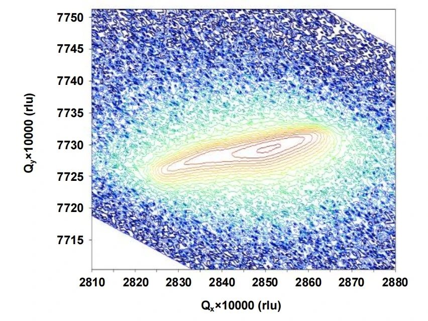
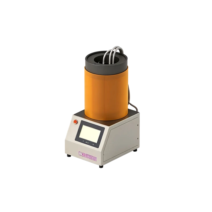
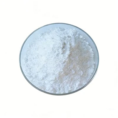
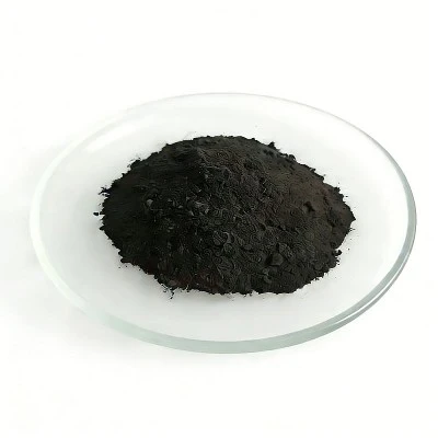
Aluminum gallium nitride (AlGaN) is a key semiconductor material for UV LEDs because its adjustable aluminum composition determines the bandgap and supports different ultraviolet emission wavelengths, while aluminum nitride (AlN) provides an important substrate or template for epitaxial growth using processes such as MOCVD and HVPE. Advanced epitaxial engineering must control aluminum composition, layer uniformity, and crystal defects, with pyramid nano-patterned substrate (NPSS) technology helping reduce dislocation density to approximately 3 × 108 cm-2 and providing a stronger material foundation for high-performance UV LED chips.
Chip Architecture Converts Epitaxial Properties into Electrical and Optical Output
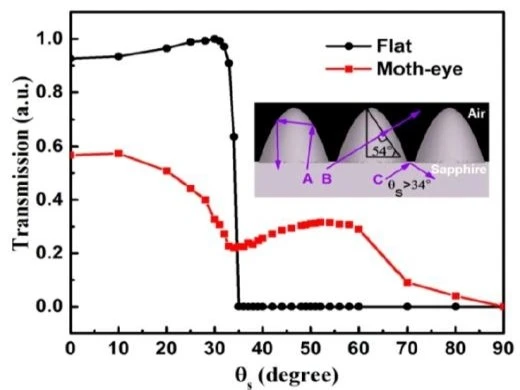
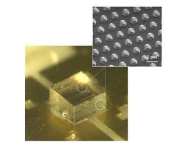
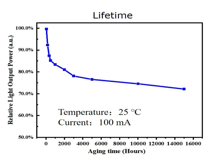
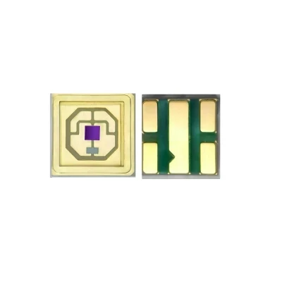
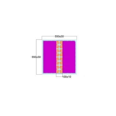
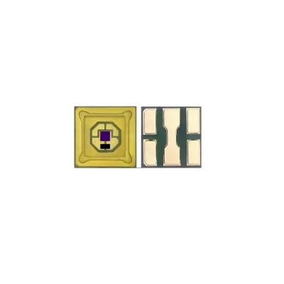
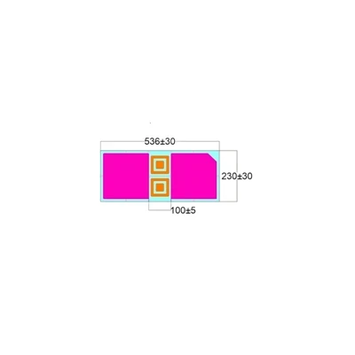
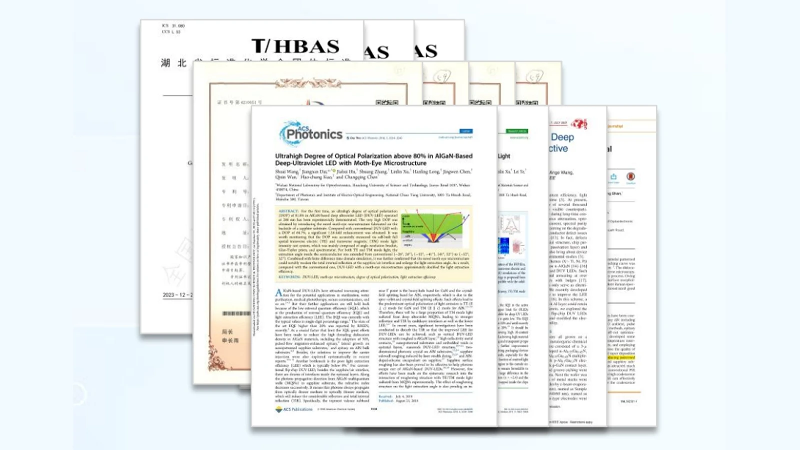
After epitaxial growth, chip architecture determines how effectively the semiconductor converts electrical input into UV emission, with active-region design, electrode configuration, and current distribution influencing electrical behavior and optical output, while moth-eye microstructures and omnidirectional reflection (ODR) structures improve photon management by enhancing TE- and TM-mode light extraction. Advanced AuSn eutectic flip-chip technology supports reliable electrical interconnection, while high-performance chip designs can achieve optical output above 60 mW at 100 mA, wall-plug efficiency (WPE) above 13.6%, and an L70 lifetime exceeding 15,000 hours under specified test conditions, demonstrating how material and chip engineering translate into measurable device performance.
Thermal & Optical Engineering: Turning Chip Output into Usable Module Performance
The chip's optical and electrical characteristics do not automatically translate into consistent module performance, making thermal and optical engineering essential for controlling operating stability and radiation output.
UV LED Thermal Management Controls Junction Temperature
Because part of a UV LED's electrical input becomes heat, thermal management must control junction temperature to limit its effects on optical output, emission characteristics, and long-term reliability. Engineers need to evaluate the complete heat-transfer path, including AuSn eutectic flip-chip bonding, die-attach interfaces, substrate conductivity, PCB layout, and heat-dissipation structures, while flexible fluoropolymer packaging can provide another packaging option for high-power UV LED components, with thermal simulation and prototype measurements helping verify actual operating conditions.
UV LED Optical Design Shapes the Module's Radiation Output
The module's radiation field depends on how individual chips are arranged and combined with optical components, including lenses, reflectors, beam angles, and chip spacing, which together determine irradiance distribution and effective coverage. Available viewing-angle configurations such as 30°, 60°, and 120°, as well as optional UVC+UVA dual-chip arrangements, provide different optical integration possibilities, while optical simulation and irradiance measurements help engineers select suitable configurations for defined working distances, target areas, and radiation requirements.
UV LED Module Development & System Integration: From Components to Complete Equipment
Once thermal and optical requirements are defined, the next challenge is to translate these designs into compatible hardware and integrated equipment through coordinated module development and system engineering.
UV LED Module Development Integrates Multiple Hardware Components
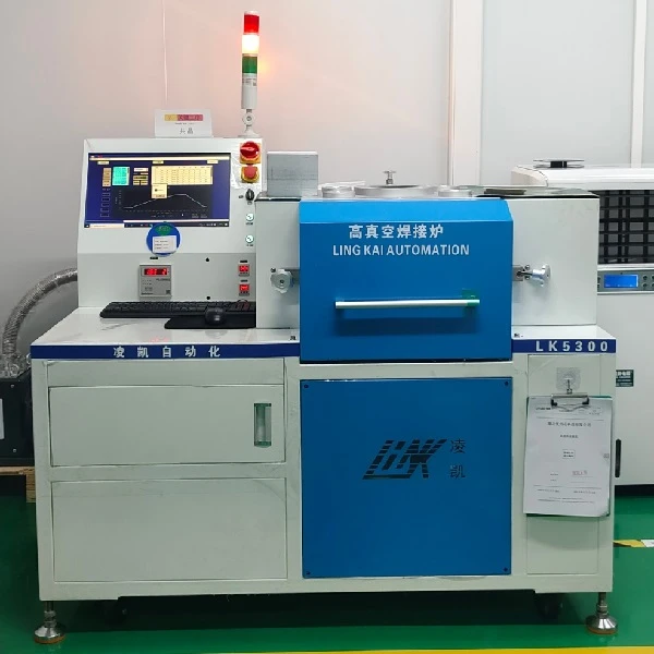
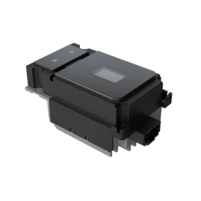
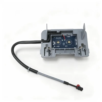
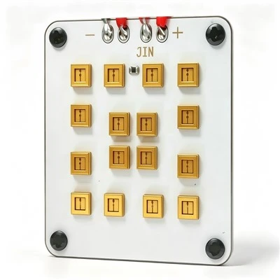
A UV LED module combines light sources with supporting hardware such as PCBs, constant-current drivers, thermal structures, optical components, and, where required, sensors or monitoring elements, with package dimensions and electrical configurations selected according to the intended equipment. Manufacturing these modules requires coordination across chip selection, AuSn flip-chip or other suitable packaging processes, PCB assembly, SMT, and mechanical integration, ensuring that component interfaces, power requirements, installation positions, and operating conditions are compatible within the finished module.
UV LED System Design Connects Modules with Equipment Architecture
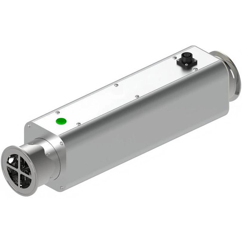
System integration connects the module with the equipment's electrical architecture, mechanical structure, control logic, and operating interfaces, including power supply, sensor signals, communication, circuit protection, and equipment-level control requirements. Engineering teams can combine optical modeling and CFD analysis where relevant with in-house laboratory testing, prototype assembly, and system validation to assess whether the complete equipment meets its intended structural, electrical, and operational requirements before production.
UV LED Application Engineering: Translating System Design into Real-World Performance
A properly integrated system provides the hardware foundation, but its performance must still be evaluated against the operating conditions and functional requirements of each application, since different processes require different wavelengths, radiation characteristics, and equipment configurations.
1. High-Flow Water Disinfection Requires Consistent UV Dose Delivery
High-flow water disinfection depends on delivering an adequate and consistent UV dose, which is affected by water transmittance (UVT), flow rate, reactor geometry, and the distribution of water velocity within the treatment chamber. CFD and optical-field analysis can help identify uneven flow paths and low-exposure areas, while system validation must confirm treatment performance under defined operating conditions, including high-throughput configurations rated at up to 120 t/h where specified.
2. All-LED Curing Requires Matching Radiation Output with Production Processes
Industrial All-LED curing requires the LED wavelength and irradiance to match the photoinitiators and materials used in inks, adhesives, and coatings, making UVA wavelength selection a central part of process adaptation. Engineers must also consider effective curing width, working distance, conveyor speed, and exposure time, then verify curing consistency through trials using representative materials and actual production conditions rather than relying on nominal optical output alone.
3. Automotive and Home Appliance Applications Require Compact and Safe Integration
Automotive and home appliance applications require UV LED modules to fit restricted installation spaces while meeting electrical, temperature, vibration, airflow, and user-safety requirements, with potential uses including cabin air treatment, high-touch surface disinfection, and integration into air conditioners, air purifiers, washing machines, and refrigerators. Engineers must define mounting positions, operating states, exposure protection, and relevant monitoring or interlock functions, while functional materials such as MOFs-TiO₂ and MOFs-MnO₂ may offer potential opportunities for combining adsorption or catalytic functions with UV technologies in application-specific development.
Commercial Values of Full-Chain UV LED Engineering: Beyond Component Supply
Meeting different application requirements depends not only on individual components but also on how effectively engineering, manufacturing, testing, and production planning are coordinated across the entire development chain.
Fewer Technical Interfaces Across the Supply Chain
When epitaxial materials, chip fabrication, packaging, module production, and system integration involve separate suppliers, buyers must coordinate multiple technical teams and resolve compatibility issues across different development stages. A vertically integrated engineering partner can reduce these interfaces by connecting the relevant manufacturing and technical processes, improving communication, maintaining greater consistency between specifications, and providing clearer responsibility when issues arise between components and finished equipment.
More Efficient Product Development and Customization
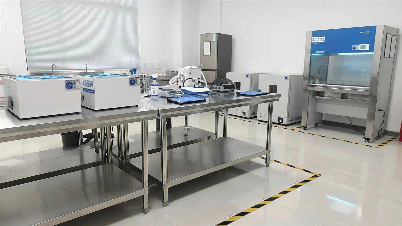
Changes to wavelength, optical output, package dimensions, viewing angle, module interfaces, or operating conditions can require repeated coordination when different suppliers manage each development stage independently. Access to in-house R&D, material and device testing, optical and thermal evaluation, and module-level validation provides a more connected basis for assessing customization feasibility and understanding how design changes may affect downstream product performance.
Better Continuity from Prototype to Mass Production
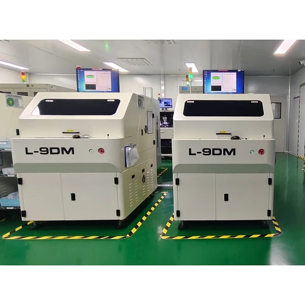
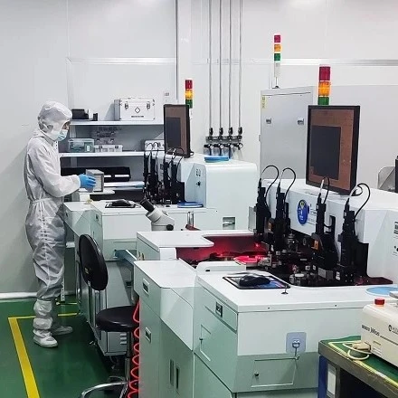
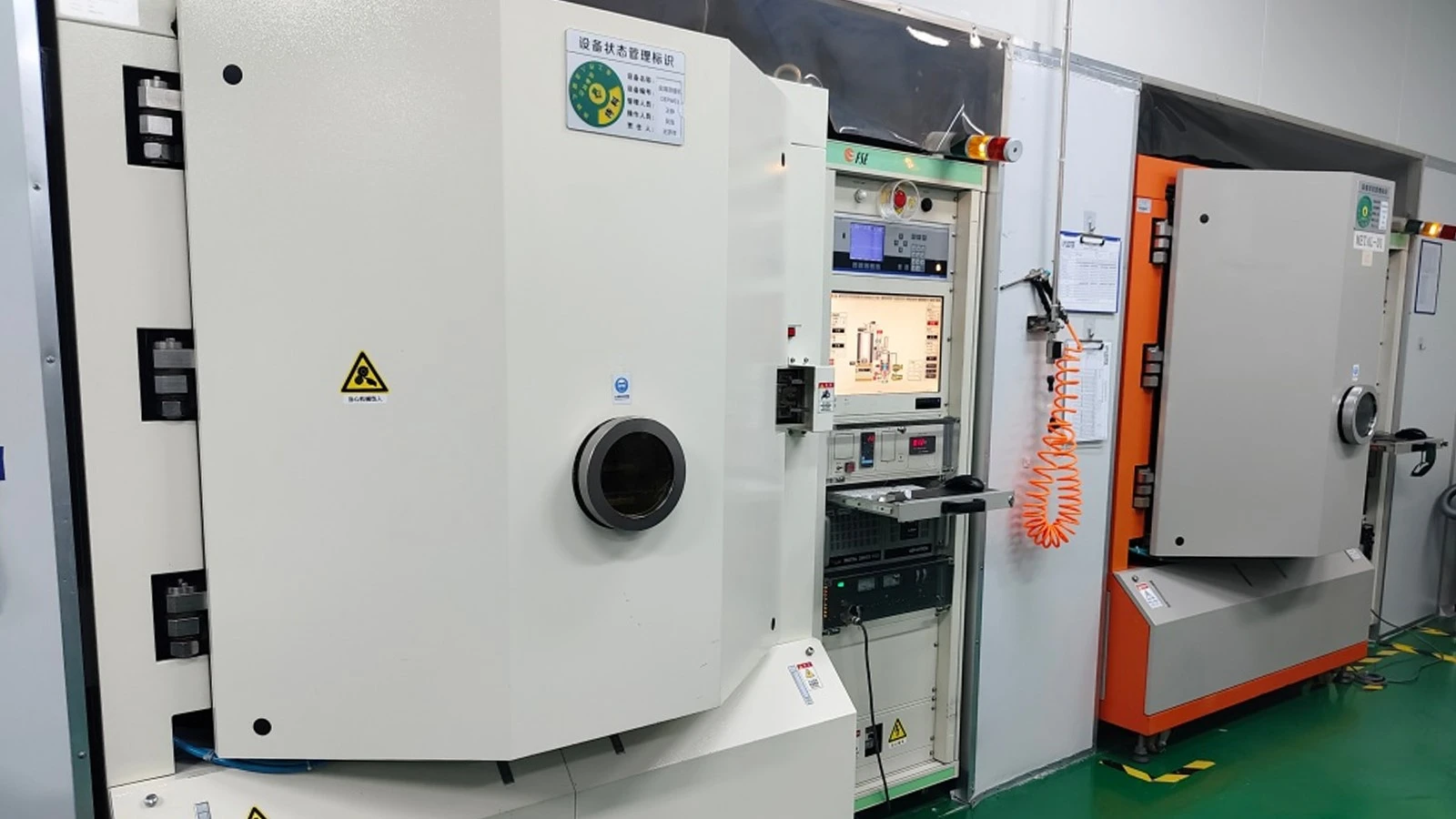
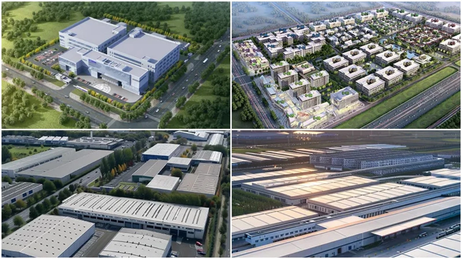
Moving from a successful prototype to consistent mass production requires continuity in chip specifications, packaging processes, assembly requirements, testing methods, and acceptance criteria, supported by manufacturing resources capable of handling different development and production stages. Coordinated chip fabrication, packaging, SMT, module and system assembly, laboratory validation, and specialized production bases help maintain technical consistency between validated samples and production units while providing a more stable foundation for future product iterations.
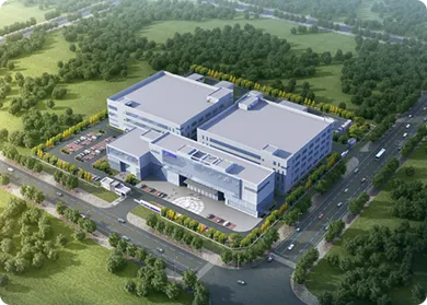
UVLEDTEK integrates in-house capabilities across epitaxial growth, UV LED chip fabrication, device packaging, testing, module manufacturing, and application-specific system development. Its vertically integrated production chain connects optical, thermal, electronic, and application engineering to support customers from initial product requirements through validation and volume manufacturing.
Why Choose UVLEDTEK as Your UV LED Manufacturer
Conclusion
UV LED performance develops through a connected engineering process in which semiconductor materials establish the foundation, chip and packaging technologies determine device performance, and module and system engineering prepare the technology for real operating conditions. For equipment manufacturers and project developers, working with a full-chain technical partner can help connect these stages and reduce the gaps between component specifications, product development, and application requirements. Contact our technical team with your target application, required wavelength, optical output, operating conditions, and system specifications to discuss a UV LED solution for your project.
Find a Tailored UV LED Solution