Introduction
As UVC LED systems become more compact and powerful, thermal management increasingly determines whether a design can maintain its target optical output and operational reliability. Because much of the electrical input is converted into heat rather than ultraviolet radiation, densely integrated LEDs can develop localized hot spots inside water-treatment modules, HVAC equipment, and sealed household appliances. Without a properly engineered thermal path, rising junction temperature can reduce UVC LED output, accelerate lifetime degradation, and compromise overall system performance.

How Junction Temperature Affects UVC LED Output and Lifetime
Junction temperature directly influences the optical efficiency, wavelength stability, and long-term reliability of a UVC LED, making it a critical parameter during device selection and thermal design.
The Thermal Feedback Loop Between Efficiency and Heat Generation
- Temperature-Dependent Efficiency: As junction temperature rises, temperature-sensitive carrier recombination and semiconductor processes can reduce optical conversion efficiency, causing a smaller proportion of electrical input to become useful UVC radiation.
- Increasing Heat Dissipation: When optical output decreases at a comparable electrical input, a greater proportion of the supplied energy is dissipated as heat, potentially increasing junction temperature further if the cooling system cannot remove it.
- Current and Thermal Interaction: Increasing forward current from 160 mA to 350 mA or 600 mA can increase optical output, but the resulting thermal load and efficiency droop must be evaluated using the specific LED's electrical and thermal characteristics.
How Junction Temperature Reduces UVC LED Output
- Radiant Power Reduction: At a fixed drive current, elevated junction temperature can reduce radiant power, so engineers should measure optical output after thermal stabilization rather than rely exclusively on room-temperature specifications.
- Peak Wavelength Shift: Temperature changes can shift the emission spectrum away from its nominal wavelength, making it important to verify that a device designed for the 260–280 nm UVC band maintains suitable spectral performance under actual operating conditions.
- System-Level UV Dose: Lower optical output can reduce the irradiance reaching the target, while the delivered UV dose also depends on exposure time, optical geometry, water transmittance, and flow conditions in water-treatment applications.
Engineers should characterize radiant power and peak wavelength across the intended current and temperature range, using consistent measurement conditions to distinguish electrical effects from thermal effects.
How Thermal Stress Accelerates UVC LED Lifetime Degradation
- Arrhenius Lifetime Relationship: The Arrhenius model describes how the rate of a specified thermally activated degradation mechanism increases with temperature, but quantitative lifetime predictions require a validated activation energy and relevant device-aging data.
- Package and Interconnect Degradation: Repeated temperature changes and prolonged thermal stress can contribute to package-interface damage, solder-joint fatigue, and other failure mechanisms that reduce reliability or eventually interrupt electrical operation.
- L70 Lifetime Verification: L70 represents the time required for optical output to decline to 70% of its initial value under defined conditions, so a specification such as 15,000 hours at L70 should be interpreted alongside the applicable model, drive current, temperature, and test methodology.
- Reliability Testing: Long-term aging tests, periodic optical measurements, and thermal monitoring help engineers determine whether a device maintains its expected output over time rather than relying solely on theoretical lifetime calculations.
Reducing junction temperature can help control thermal stress, but it does not guarantee a particular L70 lifetime because material degradation, current density, packaging, and operating conditions also influence the outcome.
Designing a Low-Thermal-Resistance Path From Package to System
An effective thermal design must control resistance across the complete path from the semiconductor junction through the package, solder joints, PCB, thermal interface, and heat sink rather than optimize any component in isolation.
Select an LED Package That Supports the Thermal Load
- Flip-Chip and Bonding Technology: Flip-chip structures can shorten the thermal path through the chip contacts, while suitable eutectic bonding processes can provide reliable thermal and electrical connections when the materials and manufacturing process are properly controlled.
- Thermally Conductive Substrates: Aluminum nitride typically offers thermal conductivity around 140–180 W/(m·K), compared with approximately 20–30 W/(m·K) for alumina and 0.2–0.4 W/(m·K) for conventional FR-4, although actual values depend on material grade and construction.
- Package and Current Selection: When comparing 3535 and 6565 packages or evaluating operation at 350 mA and 600 mA, engineers should verify the exact model's thermal resistance, maximum junction temperature, recommended PCB layout, and permitted electrical operating conditions.
A package's material conductivity alone cannot establish its overall thermal performance because die attachment, package geometry, contact interfaces, and board construction also contribute to effective thermal resistance.
Optimize PCB Integration and Thermal Interface Materials
- PCB Thermal Path: Metal-core PCBs can improve heat spreading in compact assemblies, but dielectric thickness, dielectric conductivity, copper geometry, mounting surfaces, and the connection to the heat sink must be evaluated together.
- Thermal Interface Material Control: Excessive thermal grease or pad thickness, uneven contact pressure, contamination, and trapped air can increase interface resistance and create localized hot spots even when the heat sink itself is adequately sized.
- Solder-Joint Inspection: Voids beneath thermal pads reduce the effective heat-transfer area and can produce uneven temperature distribution, so acceptance criteria should follow package-specific requirements, process capability, and reliability validation rather than a universal void-rate limit.
- Assembly-Level Validation: Temperature measurements and optical output tests should be performed on representative assembled modules to identify bottlenecks that cannot be detected by evaluating the LED package alone.
Size the Heat Sink for the Actual Operating Environment
- Passive and Forced-Air Cooling: Natural-convection designs require sufficient surface area and suitable fin spacing, whereas forced-air systems must account for airflow direction, fan performance, pressure drop, and the possibility of dust accumulation.
- Water-Cooling Design: Flowing water can remove heat efficiently when the LED board is properly coupled to a conductive housing, but the result depends on water temperature, flow rate, wetted surface area, and interface resistance.
- Junction Temperature Estimation: A first-order estimate uses the formula below, where ambient temperature, dissipated heat, and the applicable effective thermal resistance determine the estimated junction temperature.

- Simulation and Measurement: Thermal simulation can identify hotspots and compare heat-sink geometries, but engineers should validate the model against prototype measurements under representative operating conditions before finalizing the design.
For a multi-layer thermal path, each relevant resistance should be evaluated according to its boundary conditions, and heat dissipation should be distinguished from total electrical input when a meaningful portion of the input becomes optical radiation.
Prevent Thermal Coupling in High-Density and UVC+UVA Designs
- Array Spacing: Closely packed emitters can create overlapping thermal fields, so engineers should evaluate LED spacing, board-level heat spreading, and the resulting temperature distribution across the complete array.
- Cumulative Heat Loading: Thermal models should account for the combined heat generated by all simultaneously operating chips rather than estimating each LED independently.
- UVC+UVA Integration: When UVC and UVA emitters share a package or PCBA, suitable placement, heat spreading, and thermal-path management can reduce unwanted thermal coupling between channels.
- Operating-Mode Validation: Continuous operation, pulsed operation, and simultaneous UVC/UVA activation should be evaluated where applicable because the highest junction temperature may occur under a different condition from the highest instantaneous optical output.
Thermal Management Strategies for Different UVC LED Applications
Application-specific thermal design must account for the surrounding medium, installation constraints, electrical safety requirements, and required optical output because water-treatment modules and enclosed air-purification equipment experience different heat-transfer conditions.
Flowing-Water Disinfection Modules
- Conductive Housing Design: A copper or suitable stainless-steel housing can transfer heat from the LED assembly to the water-contacting surface, although the final material choice must balance thermal conductivity, corrosion resistance, structural requirements, and water compatibility.
- Flow and Temperature Control: Engineers should assess inlet-water temperature, flow rate, pressure drop, and flow distribution because insufficient local flow can cause hotspots even when the average water temperature appears acceptable.
- Electrical and Environmental Protection: Sealing, insulation, corrosion control, and condensation management must be validated to prevent moisture-related electrical failures during operation.
- Worst-Case Testing: Thermal stability and optical output should be verified at the highest expected inlet-water temperature, minimum permitted flow rate, and maximum intended LED loading.


Static-Water, HVAC, and Household-Appliance Applications
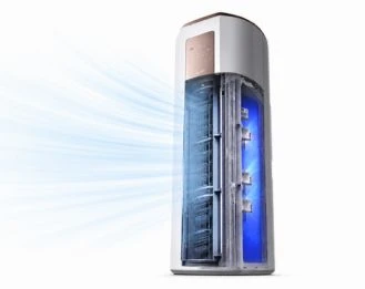
- Passive Heat Dissipation: Compact equipment may require optimized heat-sink surface area, fin spacing, and orientation because limited airflow restricts natural convection.
- Enclosure Temperature: Thermal analysis should account for heat generated by nearby electronics, elevated internal ambient temperature, and restricted airflow rather than treating the LED as an isolated component.
- Drive Current and Duty Cycle: Operating at 40–200 mA may reduce heat generation compared with higher-current operation, but engineers must confirm that the resulting optical output still meets the application's validated performance requirements.
- Moisture and Condensation Protection: Chilled HVAC assemblies and static-water equipment require suitable sealing, insulation, and electrical protection to manage condensation risks alongside thermal performance.

See Our Home Appliance/HVAC Solutions
UVLEDTEK provides UVC LED product options and system ODM engineering support relevant to thermal simulation, fluid-flow analysis, module integration, and reliability validation, helping engineering teams assess thermal constraints across the device and application. For projects requiring customized integration, engineers can prepare the target optical output, drive conditions, duty cycle, ambient temperature, installation dimensions, cooling method, and PCB layout to support a more application-specific design evaluation.


Conclusion
Thermal management directly affects UVC LED output, wavelength stability, and lifetime, making it a core design requirement rather than a corrective measure added after integration. Engineers should evaluate the complete thermal-resistance network and validate performance through device-specific specifications, thermal simulation, prototype measurements, and appropriate reliability testing. Review the relevant electrical, optical, and thermal parameters for your target application and request engineering support to develop a UVC LED integration solution that meets your performance and lifetime requirements.
Explore Your UVC LED Integration Solution