UVLEDTEK R&D team "Progress in UV luminescent chips" Reported successively by international authoritative semiconductor publications
technological leadership, Better product!
Semiconductor deep ultraviolet light-emitting diode chip for single-chip integrated photomultiplier converter
Monolithic integration of deep ultraviolet LED with a multiplicative photoelectric converter
Chen Changqing, Dai Jiangnan's R&D team will be the first to p-i-n Single chip integration of detection structure in deep ultraviolet LED In the chip, Implemented carrier cycle injection, Optical multiplier amplification function, obtained 21. 6%The highest international electro-optical conversion efficiency value.
For a long time, Semiconductor deep ultraviolet LED Although technology is widely regarded as promising, But due to its photoelectric conversion efficiency, it has never been able to break through 10%, Wandering in the primary stage of commercial application, it is difficult to move forward, Its energy efficiency, environment protection, portable, long lifespan, Widely applicable to medical phototherapy, Sterilization, air purification, confidential communication, The market potential of gas detection cannot be unleashed.
Regarding this, Riken Institute H. Hirayama research team, Technical University of Berlin, Germany C. Kuhn The research team has successively proposed using an electron blocking layer to suppress electron leakage, Using tunneling junctions instead P Various methods such as improving hole injection efficiency through aluminum gallium nitride layer, No breakthrough progress has been made.
Chen Changqing, The research and development achievements of the Dai Jiangnan team have solved this international problem.
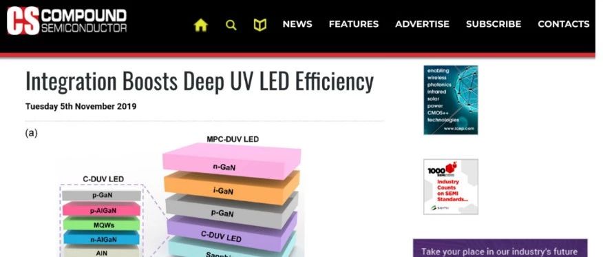
Single-chip integration technology, It is the integration of two or more devices or functional structures into a single chip, And utilize their interactions to improve the performance of the equipment. in essence, This system level innovation can create a new device environment, implement "On-chip system" . Chen Changqing, Dai Jiangnan's research team proposed a new idea of introducing single-chip integration technology, Translate into English p-i-n In situ growth of gallium nitride detection structure in deep ultraviolet light LED On the epitaxial structure (MPC-DUV LED: Monolithic integration of deep ultraviolet LED) , Realize carrier circulation injection, Chip devices with photomultiplier amplification function.
Chen Changqing, Dai Jiangnan's team conducted extensive research and exploration over a long period of time, Innovatively incorporating p-i-n The detection structure is applied in deep ultraviolet light LED In the chip, The emission from the active region of a quantum well can be 280 nm The following deep ultraviolet light absorption, And converted into new electron hole pairs. Under the action of external high voltage, The generated electron hole pairs undergo separation, Drift of hole carriers in the direction of vector wells under the action of an electric field, And re inject it into the quantum well.
Research finds, Under low current conditions, tradition DUV LED The chip operates in a current driven mode, Its output power shows a linear increase. Unlike it, MPC-DUV LED The chip operates in a voltage driven mode, Its output power increases exponentially.
Further research reveals that under low current conditions MPC-DUV LED The mechanism by which chips achieve ultra-high conversion efficiency. pass APSYS simulation calculation, i-GaN The electric field in the layer can reach 5×10⁶ V/cm, Exceeding the threshold electric field of Geiger mode in gallium nitride materials (2. 4~2. 8×10⁶ V/cm) , Therefore, there is a high probability of collision ionization occurring in the depletion layer, Obtain high gain of tens or even hundreds of times, Thus achieving an increase in the order of magnitude of hole carriers.
During the entire photoelectric cycle, electrons and holes in the quantum well undergo recombination and emit light, A portion of deep ultraviolet photons escape from the bottom of the device, Another part of the photons enter MPC Absorbed in the structure, High energy deep ultraviolet photons excite gallium nitride materials to generate corresponding electron hole pairs, And separation occurs under the condition of applied voltage, Under the strong electric field in the depletion region, holes undergo collisional ionization, After multiple multiplications, it is re injected into the quantum well, New radiative recombination occurs with the existing electrons in the quantum well, Such a cycle, Ultimately, the carrier injection efficiency was significantly improved.
Chen Changqing, The Dai Jiangnan team 2008 Joined the Wuhan Optoelectronics National Research Center of Huazhong University of Science and Technology in (Former Wuhan National Laboratory of Optoelectronics (plan) ) Since its establishment, We have been focusing on the exploration and research of semiconductor deep ultraviolet light-emitting chip devices.
In recent years, at AlGaN (AlN) Epitaxial growth of core materials (The high-quality prepared among them AlGaN Epitaxial core material, Assisting 2018 year 09 moon 07 China Ocean One C The satellite played an important role in the successful launch) ( Crystengcomm, 21, 4072-4078, 2019; Applied Physics Letters, 114, 042101, 2019) , chip design (ACS Photonics, 6, 2387-2391, 2019; IEEE Electron Device Letter, 2948952, 2019; Optics Express, 27, A1601-A1604, 2019) , fabrication of devices (ACS Applied Material Interfaces, 11, 19623-19630, 2019; IEEE Transaction on Electron Devices, 65, 2498-2503, 2018) Exploring new structures and mechanisms (Nano Energy, 104181, 2019; Optics Letter, 44, 1944-1947, 2019) A series of scientific research has been conducted in various aspects.
Published by the Chinese Academy of Sciences JCR Zone 1 paper 10 piece, Approved national level project 12 item (The National Key Basic Research Development Program 973 Project topic (Including sub topics) 2 item (N0. 2010CB923204, 2012CB619302) , Major sub project of the National Natural Science Foundation of China 1 item (N0. 10990103) , National Key Program Research and Development Project (Including sub topics) 3 item (No. 2018YFB0406602, 2016YFB0400901, 2016YFB0400804) , General Fund Projects 4 item (No. 61774065, 60976042, 61675079, 61974174) , Youth Fund Project 2 item (No. 51002058, 61704062) .
Paper link:
https: //pubs. acs. org/doi/abs/10. 1021/acsphotonics. 9b00882
https: //www. sciencedirect. com/science/article/pii/S2211285519308882? via%3Dihub
Column report link:
http: //www. semiconductor-today. com/news_items/2019/oct/kaust-301019. shtml
https: //compoundsemiconductor. net/article/109321/Integration_Boosts_Deep_UV_LED_Efficiency

