ultraviolet LED technological breakthrough: Wuhan Youweixin builds a new ecology of healthy sterilization industry, Leveraging the Blue Ocean of the Global Billion Dollar Market
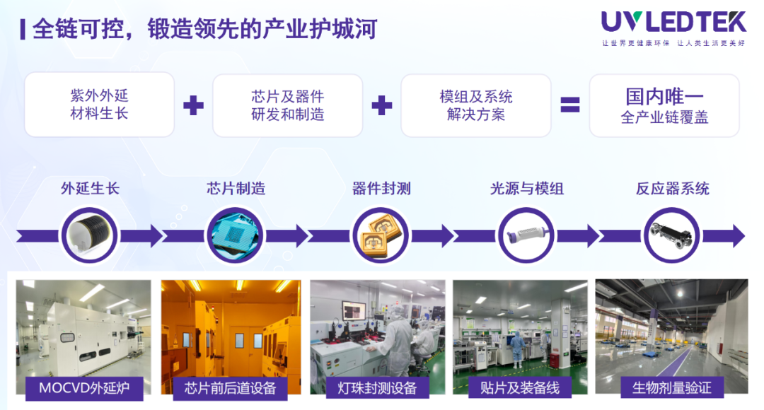
at "carbon peaking and carbon neutrality" Against the backdrop of strategic and global public health upgrading, Wuhan UVLEDTEK Co., Ltd (UVLEDTEK) In deep ultraviolet LED Breakthrough in full industry chain technology in the field, Becoming a core participant in the global semiconductor industry's innovation. As a national level specialized, refined, and innovative "Little Giant" enterprise, The company "photogene" Technological reconstruction of the healthy link between humans and the environment, Build from chip design, Vertical industry closed loop from packaging testing to scenario solutions, Promote UV LED The key leap of technology from laboratory to large-scale commercial use.
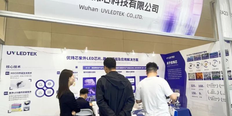
recently, at 2025 At the Jiufengshan Forum and Compound Semiconductor Industry Expo, Youweixin Technology showcased ultraviolet technology LED The latest research and development achievements of technology and their practical cases in strategic emerging industries, Triggering high industry attention.

technological breakthrough: Innovation driven efficiency leap across the entire industry chain
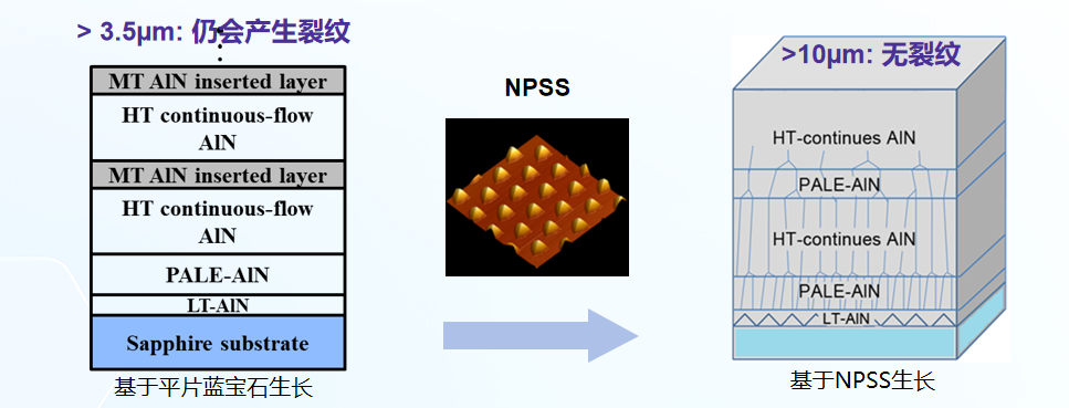
deep ultraviolet LED The core technological bottleneck lies in the efficiency of electro-optical conversion (Wall-Plug Efficiency, WPE) The industry has been consistently below 7%, Its root lies in the traditional sapphire substrate and aluminum nitride (AlN) Lattice mismatch of thin films, Causing high-density dislocations during heteroepitaxial growth, Reduce internal quantum efficiency (IQE) . Besides, AlN The thickness of the film exceeds 3. 5 When measured in micrometers, Penetrating cracks caused by stress concentration significantly reduce chip yield.
Key technological breakthroughs
01, Nano patterned substrate (NPSS) technology
Youweixin Technology introduces NPSS technology, implement AlN Lateral epitaxial growth of thin films, The dislocation density is reduced to that of traditional processes 1/3, The thickness of the film has exceeded 10 Micron without cracks, Laying the foundation for the preparation of high-power chips.
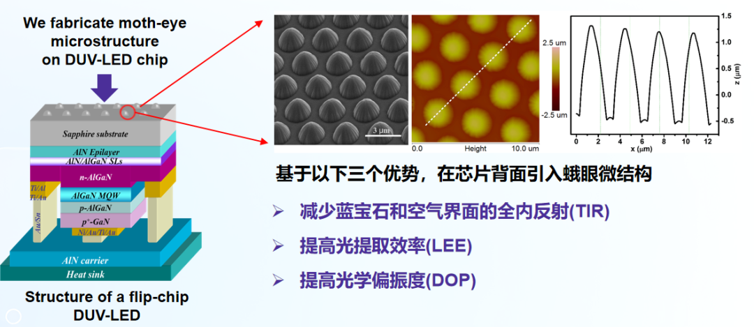
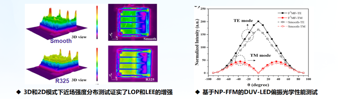
02, Optimization of Light Extraction from Moth Eye Microstructure
Drawing on the principles of bionics, Utilizing photolithography and inductively coupled plasma (ICP) etching technique, Preparation of uniform moth eye structure on the back of sapphire substrate, Extracting efficiency of deep ultraviolet light (Light Extraction Efficiency, LEE) Upgrade nearby 100%, Solved the photon problem "imprisonment" effect.
03, Flexible fluororubber nanolens packaging technology
Adopting gold tin eutectic inversion, Gaomi COB Encapsulation and flexible fluororubber nanolens array deep ultraviolet LED packaging technology, Solved the problem of poor reliability and short lifespan of devices, Develop high-power ultraviolet radiation with high light efficiency and high light power density LED Devices and Light Sources.
Construction of industrial ecology: from "Technical follow-up" to "Leading the industry" The transition
Youweixin Technology vertically integrates the entire industry chain, Breaking the international technological monopoly, Realize deep ultraviolet LED Large scale mass production of chips. Its independently developed DUV-LED chip WPE Breakthrough has been made 10% (The average international competitor is 7%) , lifespan (L70) breakthrough 15000 hour, Significantly better than industry standards.
Facing the technological barriers of international giants, Youweixin Technology Construction "independently developed+industrial synergy" The dual wheel drive mode:
01, Full chain production capacity layout
In Wuhan, Ezhou, Suzhou, Establish four major research and development production bases in Quanzhou and other places, Self built MOCVD Epitaxial furnace, chip lithography / Etching equipment, Core equipment such as automated packaging production lines, Develop a fully controllable capability for the entire process from epitaxial growth to module integration.
02, Construction of technical barriers
Accumulated patent applications 325 item (invention patent 168 item) , Breakthrough in vehicle grade reliability certification (IATF 16949) , Medical grade health license, ISO9001 Quality management and other qualification systems, Building Coverage Technology, workmanship, The three-dimensional moat of quality control.
03, Ecological strategic layout
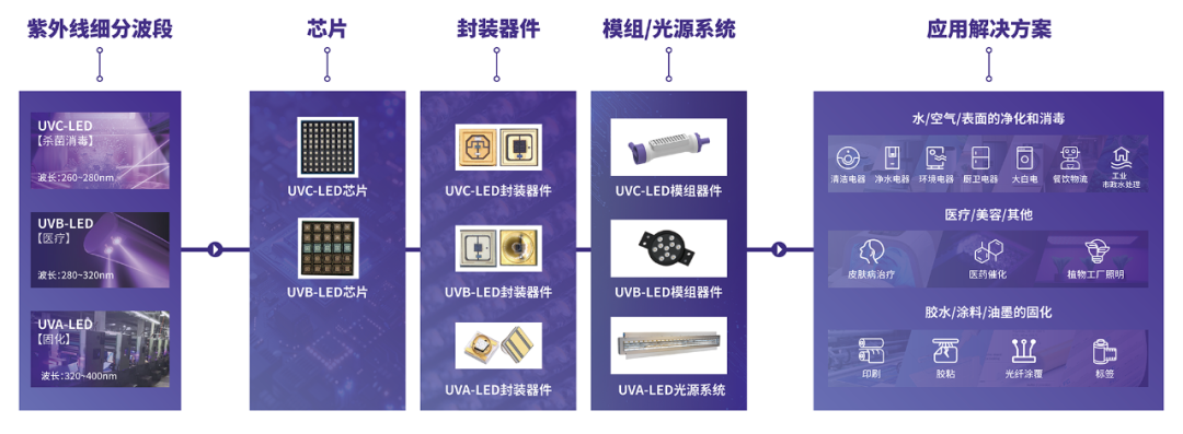
Proposed by Youweixin "1+N" Industry Matrix - With deep ultraviolet chip technology as the core, Horizontal expansion of smart home appliances, water treatment, new energy vehicle, Medical beauty, etc N An application scenario, United Beauty, Haier and other leading enterprises promote the co construction of technical standards and the implementation of scenario based solutions; Vertically based on over a decade of international leadership AlGaN ultraviolet LED Supported by R&D accumulation and industrialization experience, Quickly import into the R&D and application market layout of emerging products, Becoming a new second growth curve for company revenue.
Application scenario expansion: From laboratory to billion dollar market
As the only domestic company engaged in full band operations, A high-tech enterprise specializing in UV semiconductor chips across the entire industry chain, The core products of Youweixin Technology have excellent performance, With profound technological accumulation and continuous innovation, Widely applied in multiple key fields.
new energy vehicle: ultraviolet LED Curing technology can generate pressure resistance 3000-4000V The insulation protective film, solve 800V The problem of breakdown resistance of blue film in high-voltage batteries.
5G communication: UV light source improves fiber drawing speed 50%, energy consumption reduction 70%, Longevity achieved 30000 hour (Traditional mercury lamps 10 times) .
public health: By destroying microorganisms DNA/RNA structure, Implement for H3N2 influenza virus, Efficient disinfection and sterilization of Escherichia coli, etc, Alternative chlorine disinfection and ozone solution.
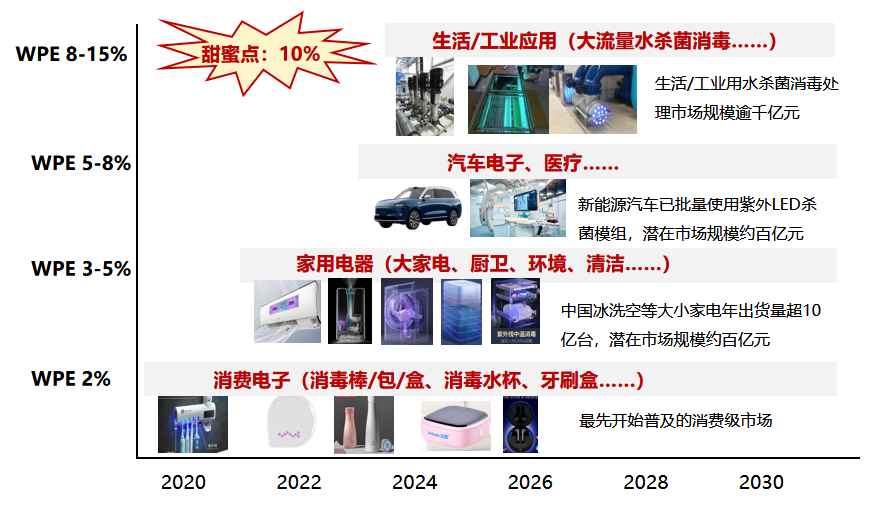
Consumption and Healthcare: Layout Air/water purification, Surface disinfection and sterilization, Scenes such as medical beauty and plant factory lighting, 2030 The market size of car mounted sterilization modules is expected to exceed 10 billion yuan in the coming year.
from China "core" To the world "chain" The Crossing
with "Minamata Convention" Comprehensive ban on mercury (2026 year) approaching, global 200 Billion dollar mercury lamp replacement market accelerates release, Youweixin Technology is about to embark on a new technological journey.
From Optics Valley's laboratory to the global industrial stage, Youweixin Technology weaves a future of health and sustainable development with ultraviolet light. As Chairman Professor Chen Changqing said: "We are not just manufacturing semiconductor devices, It is also using the power of light to reconstruct the symbiotic relationship between humans and the environment. " When UV LED Becoming the core solution for global mercury lamp replacement, When China's semiconductor technology establishes standard discourse power in emerging tracks, The growth trajectory of the enterprise, Authentic evidence of China's technological advancement "Follow the runner" to "Ecological builder" The qualitative change. at "carbon peaking and carbon neutrality" and "Healthy China" In the national strategy, Youweixin is using light as a pen, Drawing the Starry Ocean of China's Advanced Semiconductors.