Third generation semiconductor, boost "carbon peaking and carbon neutrality" goal achievement
Accelerate the independent and controllable development of the entire third-generation semiconductor industry chain


Xiaomi, Transsion and other companies are seizing the race for the application of third-generation semiconductor materials in the fast charging field; In the capital market, Third generation semiconductor upstream and downstream companies - Taiji Corporation, Antai Technology, Luxiao Technology, Haite High tech and others have shown active performance. Policy level, There are reports that, The domestic semiconductor industry will receive coordinated development, The support for industry development will also be further increased, Pay special attention to third-generation semiconductors.
In the view of industry experts such as Kunshan, Secretary General of the Third Generation Semiconductor Industry Technology Innovation Strategic Alliance, Vigorously developing third-generation semiconductors, Especially for supporting carbon peaking, Carbon neutrality is of great significance.
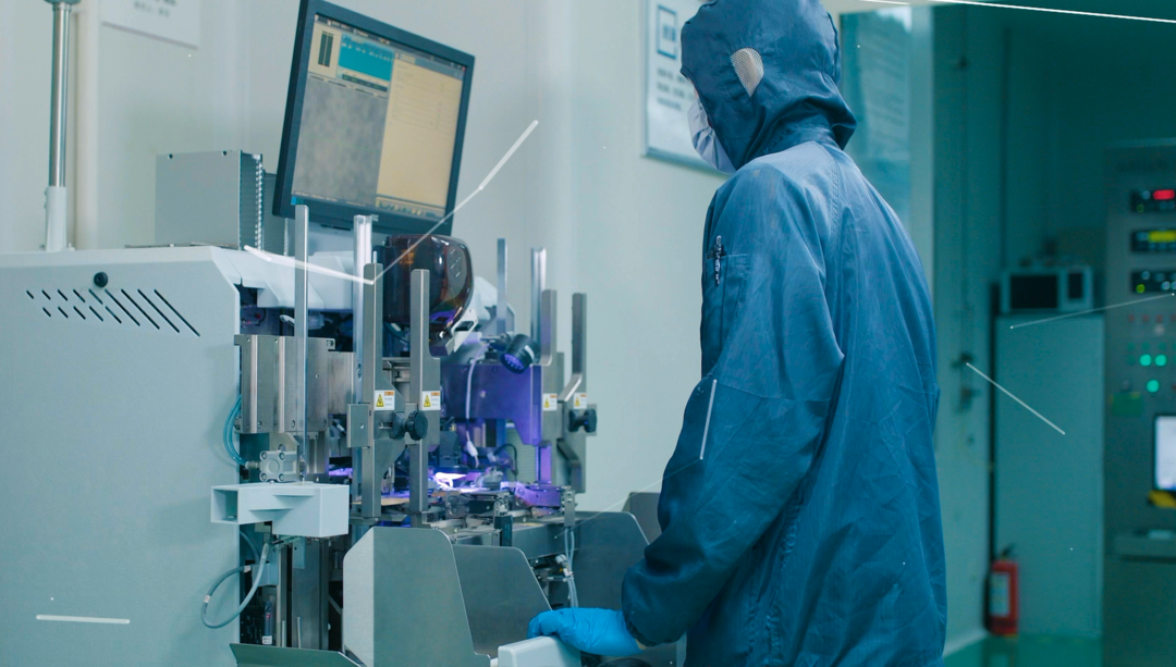
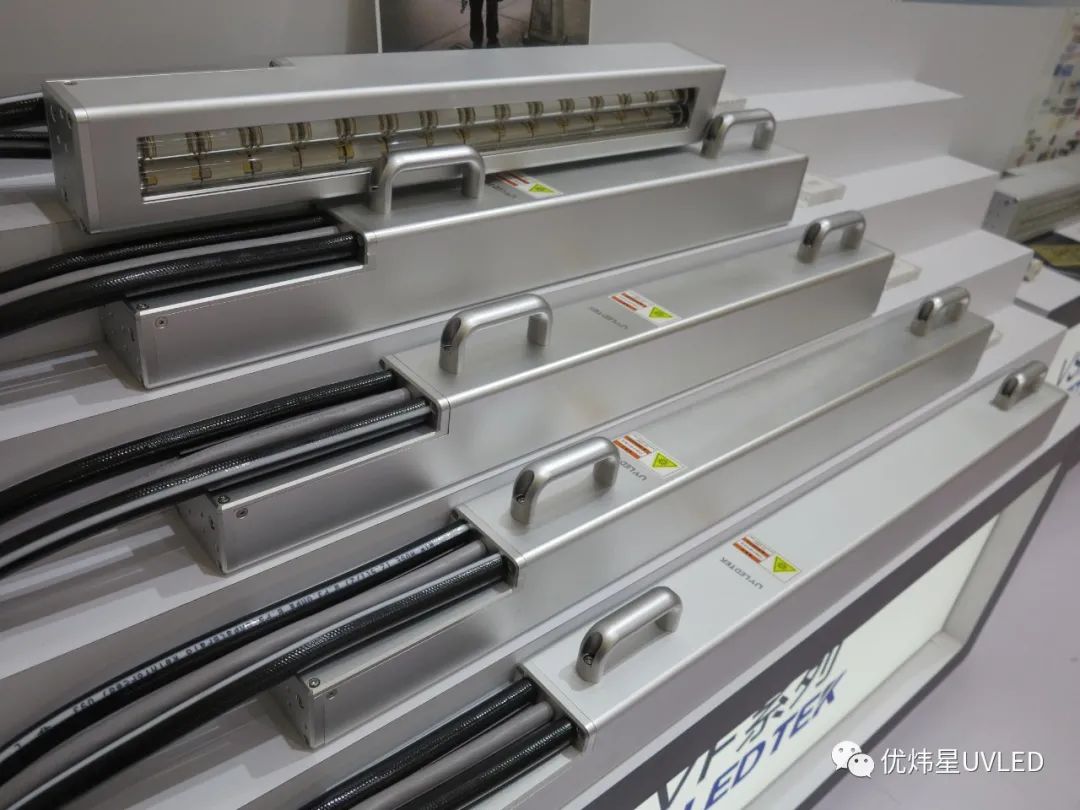
- UV LED chip packaging-
Third generation semiconductors, also known as wide bandgap semiconductors, Represented by silicon carbide and gallium nitride, Having high frequency capability, efficient, high power, high voltage resistant, high temperature resistance, Excellent performance such as strong radiation resistance.
It supports the new generation of mobile communication, new energy vehicle, High-speed rail train, Key core materials and electronic components for independent innovation, development, transformation and upgrading of energy, Internet and other industries.
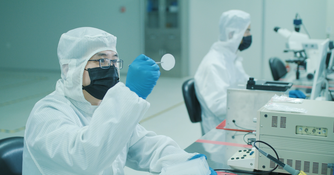
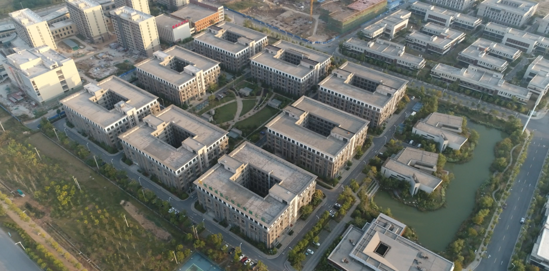
- Suzhou Extension Center -
Director of the China Electric Vehicle Hundred People's Association, Analysis by Professor Cai Wei from Harbin Institute of Technology, The inherent characteristics of third-generation semiconductor power chips and devices, Decided its role in industrial manufacturing, Advantages of efficient conversion of electrical energy in fields such as household appliances.
"Intelligent, Emerging environmentally friendly productsindustry, Urgent need for high frequency, Efficient and temperature resistant third-generation power semiconductor. " Cai Wei said.

Yu Kunshan believes that, Firstly, the key materials need to be implemented, Industrialization of core chips and modules, Optimize the layout of the industry and apply it on a large scale through demonstration and application.
Specifically, For third-generation power semiconductor devices (Two major material systems, silicon carbide and gallium nitride) demand, Accelerate the independent and controllable development of the entire third-generation semiconductor industry chain, including: Realize high performance as soon as possible 6 inch, 8 Mass production of inch silicon carbide single crystal substrates, epitaxial materials, and their power devices, 6 inch, 8 Mass production of inch silicon-based gallium nitride epitaxial materials and their power devices, Mass production of high-performance packaged devices and modules, Single crystal substrate growth, processing, chip process, encapsulation, Localization of core testing instruments and equipment for testing and other purposes.
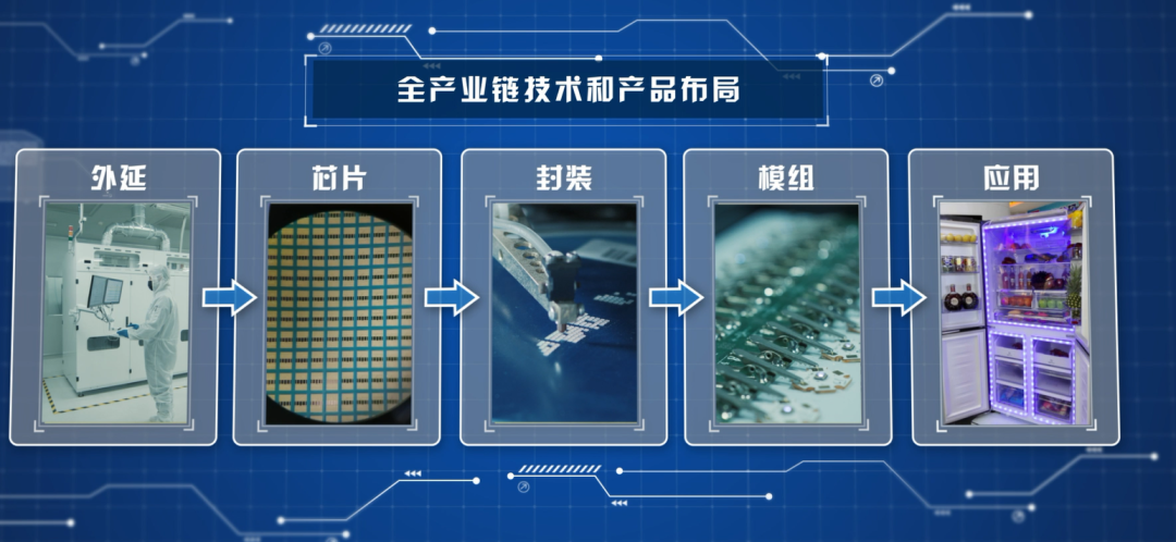
- UVA/UVC LED industrial chain layout -
Besides, Yu Kunshan's suggestion, While encouraging local governments and social capital to actively participate in the industrialization of third-generation semiconductors, We need to consider the high technological threshold of the semiconductor industry itself, Characteristics such as long cycles, Orderly promotion of industrial layout.
"Having a solid foundation in the semiconductor industry, Strong financial strength, Regions with abundant talent reserves, Gather in the industrial chainThe way to first layout upstream and midstream industries, In order to quickly achieve the industrialization of core materials and chips, Afterwards, with mature teams and enterprises as the core, Mass production and expansion on a larger scale, finallyPromote and apply mature technologies and products of third-generation semiconductors to various industries. " Yu Kunshan said.
- in-house R&D, encapsulation, production plant -
Cai Wei also emphasized, To strengthen the construction of the industrial chain, From the substrate, extension, Chip to Package, Realize low-carbon or even zero carbon strategies throughout the entire lifecycle of controller design, manufacturing, and application. "raw materials, Autonomous controllability of chips and devices is the cornerstone of the healthy development of the third-generation wide bandgap power semiconductor industry, It is also a guarantee for the implementation of the dual carbon strategy goals throughout the entire industry chain. "
- UVA LED Printing curing -
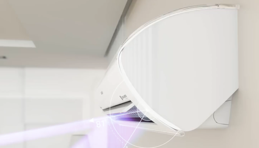
- UVC LED Sterilization appliances -
on this basis, Qiu Yufeng's suggestion, To promote the integration of research and application, Downstream white goods, consumer electronics, logistics, Carry out application demonstrations in fields such as new energy. Through application demonstration, Assist equipment manufacturing enterprises in familiarizing themselves with and mastering third-generation semiconductor devices, Accelerate the implementation of product iteration, Open the market application demand channel as soon as possible, Accelerate product maturity.


Wuhan UVLEDTEKg Technology Co., Ltd
address: Wuhan Donghu New Technology Development Zone Huagong Science and Technology Park Modern Service Industry Base 1 R&D Building B seat 5 building
postal code: 430223
Contact Number: (+86) 027-87971689
Contact email: sales@uvledtek. com (sales)